Why Contamination Control is Crucial During Semiconductor Manufacturing
Semiconductor fabrication is an exceptionally delicate and complex process, requiring atomic-level precision at every step. Even minor contamination such as temperature fluctuations, or electrical inconsistencies can compromise chip functionality. Maintaining stringent environmental controls is essential to ensure successful manufacturing.
Types of Contaminants Affecting Semiconductors²:
- Ionic materials: Chlorine, sodium, fluorine
- Molecular compounds: Vapours from greases, solvent residues, fingerprints
- Elemental particles: Copper, heavy metals, metal fibres
- Airborne particulates: Dust, skin cells, aerosols
- Physical particulates: Makeup, fibres, silicon dust
Consequences of Contamination:
- Defective products
- Reduced production yield
- Financial losses
- Increased energy consumption
- Shortened battery life
- Device failure
Six Key Steps in Semiconductor Manufacturing
Semiconductors are the backbone of every electronic device, powering everything from smartphones to spacecraft. Their unique electrical properties bridge the gap between conductors and insulators, making them ideal for controlling electrical currents in a wide range of applications.
There are six key steps in the semiconductor manufacturing process¹:
- Deposition: Wafers are sliced from a 99.9% bar of pure silicon and polished to extreme smoothness. Thin films of conducting, isolating, or semiconducting materials are deposited onto the wafer to enable the first layer to be printed on it.
- Photoresist Coating: The wafer is then covered with a light-sensitive coating called ‘photoresist’ or ‘resist’.
- Lithography: The chip wafer is inserted into a lithography machine, exposing it to deep ultraviolet (DUV) or extreme ultraviolet (EUV) light. This causes a chemical change that enables a pattern to be replicated onto the resist layer from earlier steps.
- Etching: The wafer is baked and developed, and some of the resist is washed away to reveal a 3D pattern of open channels.
- Ion Implantation: The wafer is bombarded with positive or negative ions to tune the electrical properties, enabling precise control over current flow and the creation of transistors.
- Assembly and Packaging: The wafer is diced into individual chips using a diamond saw. It is then placed onto a substrate, a type of baseboard for the chip that directs the input and output signals of the chip. A heat spreader is added to ensure the chip stays cool during operation.
Throughout these six steps, it is crucial to prevent any contamination, as even minute particles or impurities can cause defects in the chips. Take lithography, for example, a crucial step in semiconductor manufacturing. Here’s why contamination control matters:
- Photoresist defects: Contaminants can compromise the resist layer, leading to flawed patterns on the wafer.
- Pinhole formation: Dust particles can create voids in coatings, known as pinholes.
- Current flow disruption: Contaminants in conductive layers can obstruct current, causing overheating and device failure.
- Short circuits: Contaminants can cause unwanted bridging of conductive layers, leading to short circuits.
To minimize the risk of contamination, chips are manufactured in cleanrooms which provide the ultra-clean environment needed.
The Role of Cleanrooms in Semiconductor Manufacturing
Cleanrooms are controlled environments designed to minimize contamination from a range of pollutants. They maintain strict standards for temperature, humidity, air quality, and particle count, and are classified depending on the number of particles per cubic meter of air. For instance, an ISO Class 5 cleanroom must have no more than 100,000 particles smaller than 0.1 micrometres per cubic meter of air.
Cleanrooms are crucial in semiconductor manufacturing because they provide a controlled environment that significantly reduces contamination risks. By maintaining strict cleanliness standards, cleanrooms ensure high product quality, minimize failure rates, and protect business reputation and costs. They also ensure that manufacturing processes adhere to industry standards and regulations, semiconductor cleanrooms are usually required to meet ISO class 5 or lower.
To keep cleanrooms contamination-free, several contamination control measures are put in place. The industry puts a wide number of resources towards HVAC air filtration systems which use prefilters, ULPA and HEPA filters to manage contamination, however, it is important not to ignore other sources, like the floor. Studies show that 80% of contamination enters critical environments via the floor level, including on shoes or wheels.
Sources of Floor-Level Contamination
- Foot Traffic: Human activity is a significant source of contamination, with humans tracking contaminants on the sole of their shoes into controlled areas.
- Equipment Movement: Using wheeled traffic to move equipment/materials into cleanrooms can bring particles into the cleanroom on wheels or cause a stir in settled particles.
- Materials handling & Spills: Introduction of contaminants through raw materials or accidents.
- Airflow Dynamics: Air vortices can redistribute crushed particles back into the atmosphere in an erratic motion, this is called Brownian motion.
Methods for Controlling Floor-Level Contamination
Shoe Covers
Shoe covers are a traditional method for controlling floor-level contamination. Although they are widely used and can provide some benefits, they also pose several risks including:
- Inconsistent quality
- Excessive daily waste
- Particle shedding
These risks can lead to contamination entering cleanrooms, which can impact the quality and reliability of semiconductor devices, potentially leading to higher rates of defects and reduced yield.
Peel-Off Sticky Mats
Peel-off mats, also known as “sticky” or “tacky” mats, are another traditional method for controlling floor-level contamination. These mats feature an adhesive layer that captures contaminants when walked on. Once the top layer becomes saturated, it is peeled off and disposed of, to reveal a fresh adhesive layer underneath. However, studies, such as Clibbon (2002), show that these mats are only about 27% effective and have several drawbacks, including:
- Ineffective once saturated
- Redistribution of particulate into the air when peeled
- Adhesive transfer into critical area
- Excessive daily plastic waste
These disposable mats can pose a risk to cleanrooms and semiconductor manufacturing, potentially becoming a source of contamination rather than effectively preventing it.
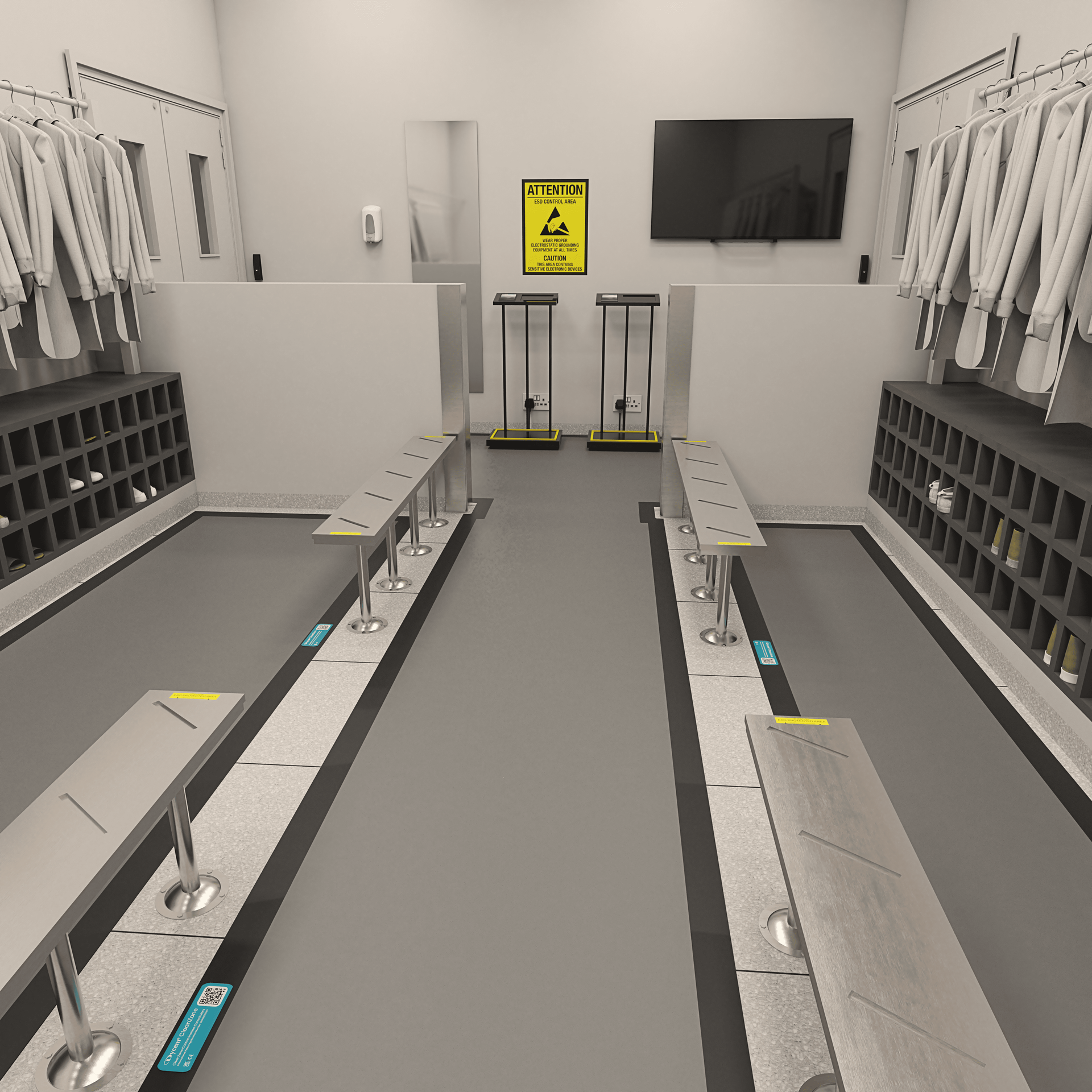
Dycem Mats
Dycem mats provide a more modern approach to floor-level contamination control. Dycem mats are crafted from a polymer with a naturally tacky surface that captures and retains up to 99.9% of contaminants from shoes and wheels, and up to 75% of airborne particulates. Here are just a few of the benefits Dycem mats can offer:
- Reusable and washable
- Lifespan of 3+ years
- Static dissipative at 108 ohms
- Customizable
- ISO compliant
Dycem offers a scientifically proven solution that effectively protects cleanrooms from floor-level contamination while serving as a more sustainable alternative to peel-off mats and shoe covers.
Benefits of Effective Floor-Level Contamination Control
- Improved yield and product quality: Fewer defects, leading to higher quality chips.
- Cost savings: Reduced wastage, rework and downtime, leading to significant cost savings.
- Extended equipment life: Minimizing contamination-related wear and tear on manufacturing tools.
- Compliance with industry standards: Meeting ISO and other cleanroom standards.
Dycem in Action
Semiconductor manufacturer onsemi turned to Dycem to address the challenge of mitigating particle ingress into their cleanroom spaces. onsemi’s experience with Dycem mats proved “outstanding,” both in terms of performance and visual appeal. The integration of Dycem significantly enhanced contamination control and safety measures for the onsemi team, offering a highly effective solution and marking a significant success for the semiconductor manufacturer.
You can read the full success story here.
Conclusion
Effective floor-level contamination control is vital in semiconductor manufacturing to ensure the highest standards of product quality and operational efficiency. The delicate nature of semiconductor fabrication demands stringent cleanliness, as even the smallest contaminants can lead to defects, reduced yield, and increased costs. Cleanrooms, with their controlled environments, play a crucial role in minimizing contamination, and managing floor-level contamination is an important part of keeping cleanrooms contamination-free.
Traditional methods like shoe covers and peel-off mats offer some benefits but also come with limitations and risks that can compromise cleanroom integrity. In contrast, modern solutions such as Dycem mats provide a more effective and sustainable approach to contamination control. With their ability to capture up to 99.9% of contaminants and a longer lifespan, Dycem mats help maintain a cleaner environment, reduce waste, and improve overall manufacturing outcomes.
By prioritizing advanced contamination control measures, semiconductor manufacturers can achieve better product quality, higher yields, and significant cost savings. Embracing innovative solutions like Dycem mats not only enhances contamination management but also supports compliance with industry standards, safeguarding the future of semiconductor manufacturing.
Get in touch with Dycem today.
References:
1 – https://www.asml.com/en/news/stories/2021/semiconductor-manufacturing-process-steps
2 – https://www.waferworld.com/post/different-types-of-contamination-that-can-affect-your-wafer